Intel vows to regain chip leadership from TSMC and Samsung by 2025Intel vows to regain chip leadership from TSMC and Samsung by 2025
Once dominant chip maker Intel shared its R&D and foundry roadmaps for the next four years, during which it plans to regain the global leader position, and unveiled two marquee customers in AWS and Qualcomm.
July 27, 2021

Once dominant chip maker Intel shared its R&D and foundry roadmaps for the next four years, during which it plans to regain the global leader position, and unveiled two marquee customers in AWS and Qualcomm.
After announcing the company’s turnaround strategy early this year, Pat Gelsinger, who came back to revitalise Intel as its CEO, revealed more detailed roadmap of what he called IDM 2.0 strategy (“integrated device manufacturer”) in the company’s “Intel Accelerated” webcast on Monday. These included new process technologies in the pipeline and planned adoption of cutting-edge packaging and manufacturing technologies.
“Building on Intel’s unquestioned leadership in advanced packaging, we are accelerating our innovation roadmap to ensure we are on a clear path to process performance leadership by 2025,” said Gelsinger. “We are leveraging our unparalleled pipeline of innovation to deliver technology advances from the transistor up to the system level. Until the periodic table is exhausted, we will be relentless in our pursuit of Moore’s Law and our path to innovate with the magic of silicon.”
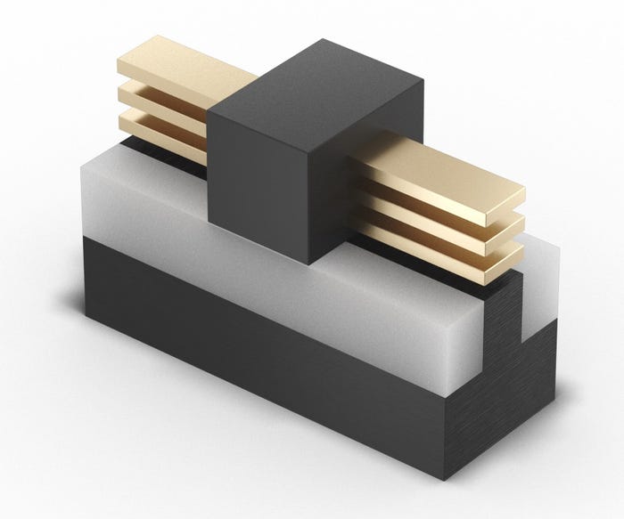
The innovation and technology advances announced at the event include new process breakthroughs. The first is RibbonFET, Intel’s first new transistor architecture since 2011 (when it unveiled FinFET). A “gate-all-around transistor”, Intel believed the technology can deliver “faster transistor switching speeds while achieving the same drive current as multiple fins in a smaller footprint.” The second key innovation highlighted by Intel is PowerVia, which Intel claims is the industry’s “first implementation of backside power delivery, optimizing signal transmission by eliminating the need for power routing on the front side of the wafer.”

Intel expects to ramp the two new technologies in 2024 and announced that Qualcomm is already on board as a customer of the new process. This should be recognised as a big win for Intel as Qualcomm has been a key customer for TSMC and Samsung.
Intel calls the new process enabled by RibbonFET and PowerVia “Intel 20A” and subsequent iterations beyond 2025 “Intel 18A”, as they will usher in the “angstrom era”. (An angstrom, or ångström, equals to 1/10 of a nanometre. Not an SI unit, the measurement, with symbol Å (reads roughly like “awe”), is named after 19th century Swedish physicist Anders Jonas Ångström.) The company said “Intel 18A” is already in development for early 2025. To make it happen Intel depends on the latest optical lithography solutions from ASML. Intel believes that it will be the first chip maker to receive the next generation production tool from the Dutch company.
Before RibbonFET and PowerVia can revolutionise processes in 2025, however, Intel needs a series of gap-filling products to play catch-up on its leading competitors. For example, it will release a new CPU for PCs later this year and a new CPU for datacentres early next year (which was delayed from this year).
By 2023, when it ships the next round of CPUs for PCs and datacentres, Intel expects to fully embrace the new circuit-printing technology, the next-generation extreme ultraviolet lithography (EUV), which Intel calls High Numerical Aperture (High NA) EUV. The company claims the new technology can deliver approximately 20% performance-per-watt increase as well as area improvements.
Somewhat confusingly, Intel decides to depart from the industry’s usual practice of naming processes by the size of transistors, for example 7nm. Instead, it is to name its improved 10nm process Intel 7, and its upcoming 7nm process, enabled by the new High NA EUV circuit-printing technology, Intel 4. Though it would be harsh to say the new naming scheme was an attempt to obscure Intel’s manufacturing issues, as an Intel executive denied to Financial Times, Intel’s own reasoning that the change will “create a clear and consistent framework to give customers a more accurate view of process nodes across the industry” is not much convincing.
Gelsinger was brought back to Intel, where he had served as CTO before leaving for EMC then VMWare, to turn around the fortune of the once world-beating chip giant that in recent years has fallen behind its Asian competitors in Taiwan and South Korea. One of his first major actions was to re-enter the foundry business. Early this month it was reported by WSJ that Intel was prepared to buy GlobalFoundries for $30 billion.
“The innovations unveiled today will not only enable Intel’s product roadmap; they will also be critical for our foundry customers,” Gelsinger said at Monday’s event. “The interest in IFS has been strong and I’m thrilled that today we announced our first two major customers. IFS is off to the races!”
Intel also shared a progressive packaging roadmap, which is a key component of its overall IDM 2.0 strategy. New packaging solutions start with near-term target of reducing bump pitch from 55-micron to 45-micron with EMIB, all the way to direct copper-to-copper bonding with Foveros Direct that aims to achieve sub-10-micron bump pitches. Intel reveals that AWS has become the first customer of Intel foundry’s new packaging solutions.
Not all questions related to Intel’s future are answered though. After Gelsinger slammed the US government’s subsidies to TSMC to build a foundry in Arizona earlier this month, it is not clear if Intel is receiving or will receive any financial support from the federal or state coffer. Gelsinger said he didn’t need government subsidies when he unveiled the new strategy.
Also unclear is Intel’s ambition in mobile devices. Since it threw in the towel on 5G smartphone chips, mobile device has been largely absent from Intel’s public messages. Whether recruiting Qualcomm, which dominates mobile devices market, as a key customer is a substitute for its direct participation in the market, or it is a first step to engineer a re-entry, is yet to be seen.
About the Author
You May Also Like


.png?width=300&auto=webp&quality=80&disable=upscale)


_1.jpg?width=300&auto=webp&quality=80&disable=upscale)